Street Insider quotes Needham analyst Rajvindra Gill saying "OVTI has lost the image sensor socket on Apple’s next-generation iPad 3 HD to Samsung. We believe the iPad 3 will include a 5MP sensor for the back-camera and will support HD resolution. Our industry checks point to Samsung winning the socket based on price competitiveness rather than better quality/technology. Five megapixel sensors are a relatively mature technology, having existed in the marketplace for over two years, and therefore other competitors, such as Samsung, Aptina and Toshiba, have developed cost competitive sensors. On the iPhone 4S front, we still contend Sony is 100% sourced at Apple. However, OVTI is trying to ramp its BSI-2 yields to 70-80% in order to be qualified as the second source (sometime in C2Q). At this juncture, it’s still uncertain".
The full Needham report can be downloaded here. Needham adds regarding the BSI-2 yield: "Our checks indicate that OVTI’s yields on its BSI-2 8MP sensor are running at 40-50%. We believe OVTI is still trying to become the second source to Sony for the 4S in C2Q. However, we believe OVTI has to increase its yields to 70-80% in order to be considered a viable second source".
Thanks to CA for sending me the news!
Aptina Shows How to Isolate Deep PDs
Aptina's patent application US20120009723 titled "Range modulated implants for image sensors" talks about deep photodiode process and shows quite impressive PD isolation shape of a 1.1um-pitched PD extending all the way through the 4um-thick epi 66 to a heavy doped substrate 64:

The company describes the challenges in deep photodiode manufacturing: "When conventional methods are used for implanting isolation regions, it can be challenging to form very narrow and deep isolation regions. Isolation regions are typically formed by implanting ions through the openings of patterned photoresist. If very narrow openings are formed in photoresist, the walls of the openings may be unstable. Narrower openings could be formed in thinner photoresist, but thinner photoresist would limit the permissible energies used during ion implantation and resulting implants would be too shallow. Shallow isolation regions are undesirable because they would limit photodiode depth, reducing the quantum efficiency and sensitivity of the pixels."
So, the photodiode isolation implants are implemented by a set of repeating steps with complementary photoresist patterns where the boron implant penetrates through the photoresist:

The resulting deep PD isolation is composed of multiple regions 92 and 94:

SiOnyx Founder Won SPIE Green Photonics Award
Harvard University: SiOnyx Founder Eric Mazur with four his students won SPIE Green Photonics Award for Laser-assisted Manufacturing and Micro/Nano Fabrication. The winning paper was written by Eric Mazur, the Balanski Professor of Physics and Applied Physics, with graduate students Benjamin Franta (lead author), Meng-Ju Sher, and Katherine C. Phillips in the Harvard Department of Physics, and Yu-Ting Lin at Harvard School of Engineering and Applied Sciences.
The group used femtosecond laser pulses to modify and control both the chemical composition and the surface structure of silicon. These modifications affect the optical and electronic properties of the material that they called "black silicon" with a potential for use in novel photosensitive devices.
The award will be presented on January 25, 2012 at SPIE Photonics West in San Francisco.
ST Proposes Bias S&H to Reduce Noise
ST Micro patent Application US20120006973 proposes to sample bias voltages and currents and hold them between CDS reset sample and signal sample, so that any bias noise does is constant over CDS cycle and, thus, subtracted. For example, in case of pixel current bias it might look like this:

In case of some other generic bias voltage, S&H might look like this:


In case of some other generic bias voltage, S&H might look like this:
Teledyne DALSA Started Imaging Blog
Teledyne DALSA begins its Imaging Blog. So far it has just the first post starting a talk about machine vision interface standards: "It started smoothly with Camera Link more than ten years ago. Then came DCAM for Firewire, followed by GigE Vision which paved the way for GenICam (itself divided into 3 modules: GenAPI, GenTL and SFNC), EMVA1288, and now CoaXPress, Camera Link HS and USB3 Vision." I hope the blog would be updated regularly!
Plessey Image Sensors
I was slow to realize that recently re-built Plymouth and Swindon, UK-based Plessey Semiconductor started to manufacture CMOS image sensors. The Plessey brand has been re-created by combining the former X-fab and Zarlink UK facilities:

"Over 30 different CMOS Image Sensors are manufactured by Plessey ranging in size from <1MP up to wafer-scale sensors. These products demonstrate very low dark currents, high radiation tolerance and high dynamic range. By working closely with our customers, Plessey ensures leading edge performance across a range of market sectors: Automotive, Medical, Dental X-ray, Professional Digital Photography, Industrial Imaging, Gene Sequencing, Space, Security, HD TV cameras... CMOS Image Sensors manufactured by Plessey feature low dark currents, radiation tolerant processes and a range of pixel sizes from 6.7um to 125um. Sensor sizes range from 1/2” optical format to full wafer scale sensor by using 1D or 2D stitching."
Plessey PS50480 VGA sensor features 4.2um 5T global shutter pixel made in 0.18um process. The sensor's spec looks quite nice, except of large PRNU and apparent lack of microlens:
- 5T Pixel Architecture
- 0.18 µm CMOS
- 656 x 488 Pixels
- 4.2 µm x 4.2µm Pixels
- 1/5” Optical format
- 1.8V Digital Power Supply
- 3.3V Analog Power Supply
- Global Shutter
- 120fps at VGA resolution (640 x 480)
- Power Consumption: 400mW
- Full Well Charge 13500 electrons
- Conversion Gain 70 µV/electron
- Spectral response 0.16A/W
- Peak QE * Fillfactor 30%
- Fillfactor 40%
- Dynamic Range 70dB
- Fixed Pattern Noise (local) <0.20%
- PRNU (local) <10%

Aptina Announces VGA SoC for Automotive Applications
Business Wire: Aptina announces ASX340AT automotive SOC sensor for applications such as rear view cameras, blind spot monitoring and surround view without the need for additional processing chips. The 1/4-inch VGA sensor features 5.6um pixel with operating temperature range of -40ºC to +105ºC.
The ASX340AT also provides notable features such as dynamic overlay capability, which allows camera system designers to add colored graphics to the display to enhance the experience of the driver, and a crop and zoom feature enabling customization to suit a wide range of vehicle body designs. Additionally, there is an on-chip temperature sensor for dynamic system feedback and additional optical pixels to assist lens alignment during camera manufacturing.
The ASX340AT SOC will be sampling starting calendar Q1 2012. It is available in a 7.5mm x 7.5mm, 63-ball iBGA package and is AEC-Q100 qualified.
 |
| Automotive rear view with graphical overlay. |
Fraunhofer Institute Proposes Ultra-Thin Multi-Apterture Wafer Level Camera
Fraunhofer Institute offers Multi aperture camera optics on wafer level (ultra-thin camera) services, including optical design, prototyping and characterization of microoptical imaging systems for custom-specific applications. Fraunhofer achieved 1.4mm-thick camera module with F3.7 lens having 700 x 550 pixel resolution. The idea of the camera was presented in SPIE Journal of Micro/Nanolithography, MEMS and MOEMS:
"Multi-aperture optics for wafer-level cameras"
Andreas Bruckner, Robert Leitel, Alexander Oberdorster, Peter Dannberg, Frank Wippermann, Andreas Brauer
"Multi-aperture optics for wafer-level cameras"
Andreas Bruckner, Robert Leitel, Alexander Oberdorster, Peter Dannberg, Frank Wippermann, Andreas Brauer
 |
| Overview of the different types of miniaturized camera modules. A schematic sideview of the optical system is shown on top of each field and a view on the image sensor on the bottom. |
 |
| Visualization of a braided sampling of the object space by multiple optical channels. The different colors illustrate the correlation between patches on the object plane, optical channels, and partial images in the image plane. |
 |
| Schematic cross section of the electronic cluster eye prototype illustrating the layer structure of the optical module, which is directly attached to an image sensor. Drawing is not to scale. |
 |
| Size comparison between the fully assembled electronic cluster eye with VGA resolution on the packaged image sensor and a commercial plastic VGA lens. |
Forbes: Omnivision Lost its Apple Business
Forbes looks into the just released Apple Suppliers list that constitutes 97% of Apple's spend. OmniVision is not listed, while Sony is there. Forbs writes: "The reasonable conclusion is that OmniVision has either lost all of its business to Sony or its business with Apple now is just a shadow of what it used to be".
It was reported earlier that iPhone 4S VGA front camera is Omnivision's. Probably it belongs to the non-listed remaining 3% of Apple’s procurement expenditures.
It was reported earlier that iPhone 4S VGA front camera is Omnivision's. Probably it belongs to the non-listed remaining 3% of Apple’s procurement expenditures.
poLight Technology Explained
poLight published a Vimeo video presentation by Jon Hermarn Ulvensøen, the company's Advance Technology VP, explaining the manufacturing process and advantages of TLens:
poLight Technology from polight on Vimeo.
Image Sensors 2012 Agenda Finalized
Business Wire: Image Sensors 2012 conference, formerly known as Image Sensors Europe, has officially announced its agenda. It mostly follows the unofficial version presented earlier, with most notable exceptions being the omission of presentations by Eiichi Funatsu, Senior Manager, Sensor Division, Sony and by Koichi Mizobuchi, Deputy General Manager, Imaging Technology Development, Olympus.
Still, the agenda remains pretty impressive, complemented by two workshops:
Sensors Architectures for 3D Time-of-Flight Imaging
by David Stoppa, Lucio Pancheri, Matteo Perenzoni
Fondazione Bruno Kessler, Italy
Workshop content:
Advanced Solid-State Imaging - Understanding and Improving Light Sensitivity
by Albert Theuwissen
Harvest Imaging, Belgium
Workshop content:
The conference is to be held in London, UK on March 20-22, 2012.
Still, the agenda remains pretty impressive, complemented by two workshops:
Sensors Architectures for 3D Time-of-Flight Imaging
by David Stoppa, Lucio Pancheri, Matteo Perenzoni
Fondazione Bruno Kessler, Italy
Workshop content:
- General introduction about 3D Imaging Technologies, applications and history
- ToF 3D Imaging measurement principle and systems
- Sensors based on in-pixel photo-demodulating devices with a real case study example
- Sensors based on extensive use of electronics in the pixel with a real case study example
- Figure of merits of ToF image sensors
Advanced Solid-State Imaging - Understanding and Improving Light Sensitivity
by Albert Theuwissen
Harvest Imaging, Belgium
Workshop content:
- Explaining and understanding the limitations of light sensitivity
- Cross-talk: spectral, optical, electrical
- Improving light sensitivity
- Micro-lenses
- Amorphous top-layers
- Light guides
- Back-side illumination
- Binning
- Electron Multiplication
The conference is to be held in London, UK on March 20-22, 2012.
Toshiba BSI Roadmap
A good part of Toshiba CES 2012 presentation is devoted to BSI image sensors. Toshiba presents its BSI roadmap (click to enlarge):

Some other slides from the presentation:
Toshiba BSI CMOS Image Sensors - Highlights


Some other slides from the presentation:
Toshiba BSI CMOS Image Sensors - Highlights
- Planning products up to the 24 MP for digital still camera applications and up to 16 MP for smartphones, tablets and new automotive applications
- Last announcement was for an 8 MP BSI CMOS image sensor with the industry’s smallest pixel size (1.12 micrometers) as of 7/7/2011
- Toshiba makes its BSI images sensors in house on 300mm wafers


Omnivision Launches 1.4um OmniBSI+ Pixel, 8MP Sensor
PR Newswire: OmniVision announces 8MP 1.4um pixel OV8825 sensor, the first one to use OmniBSI+ technology. OmniBSI+ represents the second-generation of the original OmniBSI technology, said to offer a 60% increase in full-well capacity, a 10% increase in QE and a 10% improvement in low-light sensitivity. This makes the OV8825 an attractive option for smartphone and tablet manufacturers to upgrade their camera from the 1st generation 8MP BSI sensor, the OV8820.
"Industry reports expect tablets to reach 250 million units globally by 2014, with a large portion of those using 8-megapixel cameras. Similarly, industry reports project that smartphones equipped with 8-megapixel cameras will see tremendous growth, with estimates ranging up to more than 500 million units in 2014," said Vinoo Margasahayam, senior product marketing manager at OmniVision, quoting June 2011 TSR report. "Given the low cost and overall performance improvements enabled by our new OmniBSI+ pixel architecture, we feel that the OV8825 is an excellent solution for manufacturers in these booming markets."
The 1/3.2-inch, 8MP OV8825 operates at 24fps in full resolution, and in 1080p video mode at 30 or in 720p mode at 60fps. A high-speed, 4-lane MIPI interface facilitates the required high data transfer rate. The OV8825's integrated scaler offers electronic image stabilization, and enables the sensor to maintain full FOV with improved SNR in 1080p video mode at 30fps. The sensor's 2 x 2 binning functionality with a post-binning re-sampling filter function minimizes spatial artifacts and removes image artifacts around edges.
The OV8825 fits into the industry standard module size of 8.5 x 8.5 mm. It is now available for sampling and is expected to enter mass production in the second quarter of 2012.
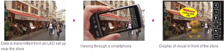
Casio Presents "Image Sensor Communication Technology"
Casio unveils "prototype visible light communication system using smartphones. The system flashes smartphone screens to achieve visible light communication (VLC). When someone takes a photo with a smartphone camera, the subjects simply turn their smartphone screens toward the camera device to display personal information or messages in the photo. The images and information are shared on the spot among everyone’s smartphones":

The same system enables users to receive information from a shop or advertiser, by viewing digital signage or an LED light source placed in front of the shop through a smartphone camera:

The Youtube video shows how the system works:

The same system enables users to receive information from a shop or advertiser, by viewing digital signage or an LED light source placed in front of the shop through a smartphone camera:
The Youtube video shows how the system works:
Omnivision Announces Native 720p/60 Video Sensor
PR Newswire: OmniVision announces 1/4-inch OV9713, the native 720p/60fps CameraChip sensor that is said to be the first sensor to be built on a new and improved OmniPixel3-HS pixel using a proven 0.11um FSI process. [It sounds like the 3 year old OmniPixel3-HS has been improved but the generation name remains same.]
The sensor's new 3um pixel offers low-light sensitivity of 3300 mV/lux-sec, better SNR and a 5dB improvement in DR compared to the previous generation. Additionally, the OV9713's 12-bit RGB RAW output capability provides optimized HDR, while the embedded sequential line- or frame-based HDR features allow an even higher DR to address high-contrast scenes often encountered indoors. The sensor is also 3D ready, offering frame synchronization functionality for 3D (stereo) camera systems. It comes with a standard 2-lane MIPI interface and fits into an 8 mm x 6 mm x 4.5 mm module size.
The OV9713 is currently available for sampling, and is expected to go into volume production by Q2 2012.

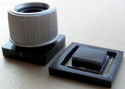
OmniBSI-2 Found inside Asus Tablet
Chipworks reverse engineering of Asus Transformer Prime tablet revealed that its primary image sensor is Omnivision's 8MP OmniBSI-2 sensor "with die markings AEQGG6 OV2B8B0 and according to the specifications the device is the OmniVision 8830". Features that show it to be BSI2 include the suspected TSVs located on either side of the bond pads (shown below) and the copper metallization found during SEM analysis.

Thanks to EK for pointing me to this!
Thanks to EK for pointing me to this!
PMD Ready for Mass Production of the First Commercially Available ToF Chip
PMD Technologies announces that is 160x120 pixel 3D FoF imager is ready for mass market usage. The PMD PhotonICs 19k-S3 is said to be the first commercially available 3D-ToF chip for camera developers and system integrators.
The read-out clocks of 15MPixel/s are said to be possible. With the integrated SBI (Suppression of Background Illumination) technology the product can be deployed in indoor and outdoor environments. Its 160x120 pixel resolution is optimized for close range human-machine interaction up to 2 meters.
PMD reference design CamBoard nano has 37x30x25mm size and is said to be the smallest depth sensor reference design available worldwide. The board is intended for near range applications, has one infrared LED as an active illumination source and is USB powered.
Providing a frame rate of up to 90fps at full resolution of 160x120 pixel with a 90deg FOV, the CamBoard nano is suitable for gesture detection. It delivers depth maps and gray value image data simultaneously.
"We are convinced that the availability of the 19k-S and the CamBoard nano reference design will initiate a 3D-ToF community, enabling applications, demos and product solutions we all don’t think of so far", says Dr. Bernd Buxbaum, CEO of PMDTechnologies. “The opportunities and use cases are endless as the PMD technology is very scalable in terms of size, performance and cost.”
Update: PMD published a flyer presenting its new small sized solution:

Canon Announces Sensor Improvements
Canon announces a number of improvements in its camcorders image sensors:
"The HD CMOS PRO sensor has evolved for the 2012 range, with refinements to the
micro lens and colour filter to allow light to be collected more effectively. An antireflection film has been added to each micro lens on the sensor whilst the colour filter material has been upgraded to a higher transmission one. The resulting low-light
performance of the sensor is 20% more effective than the HD CMOS PRO sensor
currently deployed in the HF M-series."
The large 14.3MP 1.5-inch PowerShot G1 X sensor is said to utilize on-chip noise reduction technology and has 4 channel read-out for high speed.
Fujifilm Announces X-Trans CMOS Sensor
Fujifilm announced X-Pro1 interchangeable lens camera featuring 16MP APS-C size X-Trans CMOS sensor. The sensor's color filter array "paves the way for an ideal sensor that does not need an optical low-pass filter. While the optical low-pass filter is indispensable for the reduction of moiré and false color generated by conventional sensors, it also degrades resolution.
Fujifilm has developed a new color filter array that is inspired by the random arrangement of fine film grain, removing the need for an optical low-pass filter to solve moiré and false color issues. In the array, RGB pixels are arranged in 6 × 6 pixel sets with high aperiodicity (randomness). Increasing the degree of randomness eliminates the fundamental cause of moiré and false colors — a problem that occurs in conventional arrays when shooting stripes and other repeating patterns. The presence of an R, G and B pixel in every vertical and horizontal pixel series minimizes the generation of false colors and delivers higher color reproduction".

"Moire is tackled at its root cause by the revolutionary X-Trans CMOS sensor's color filter array. By enhancing aperiodicity (randomness) in the array arrangement, the color filter minimizes generation of both moire and false colors, eliminating the necessity for an optical low-pass filter in the lens and enabling X-Trans CMOS sensor to capture full “unfiltered” lens performance."
To process the new color filter data, Fujifilm also developed EXR Processor Pro image processor.
Fujifilm has developed a new color filter array that is inspired by the random arrangement of fine film grain, removing the need for an optical low-pass filter to solve moiré and false color issues. In the array, RGB pixels are arranged in 6 × 6 pixel sets with high aperiodicity (randomness). Increasing the degree of randomness eliminates the fundamental cause of moiré and false colors — a problem that occurs in conventional arrays when shooting stripes and other repeating patterns. The presence of an R, G and B pixel in every vertical and horizontal pixel series minimizes the generation of false colors and delivers higher color reproduction".
 |
| Bayer patter repeats itself in 2 x 2 pixel units. |
| Higher degree of randomness with an array of 6 x 6 pixel units. Without using an optical low-pass filter, moire and false colors are eliminated while realizing high resolution. |
"Moire is tackled at its root cause by the revolutionary X-Trans CMOS sensor's color filter array. By enhancing aperiodicity (randomness) in the array arrangement, the color filter minimizes generation of both moire and false colors, eliminating the necessity for an optical low-pass filter in the lens and enabling X-Trans CMOS sensor to capture full “unfiltered” lens performance."
To process the new color filter data, Fujifilm also developed EXR Processor Pro image processor.
CMOSIS 2nd Patent on Ramp ADC Granted
CMOSIS announces that its second patent on ramp ADC has been granted. The US8040269 patent proposes to speedup column-level ADC converter by using just one ramp cycle to measure previously sampled column reset and signal levels:

Two counters count the clock cycles between the reference levels and the signal and reset levels, then the final value is calculated as the ratio between the two counters.

Two counters count the clock cycles between the reference levels and the signal and reset levels, then the final value is calculated as the ratio between the two counters.
Panasonic Finds Use For Polarisation Selective Pixels
Panasonic patent application US20110316983 proposes to use parallax from polarization split lens to determine the distance to the object. The lens is divided by a polarization filter into two halves:

Then the sensor has some number of pixels which are selective to the polarization, so that they get signal from only the left or the right half of the lens. Here are the examples of polarization selective pixel placement (Wv and Wh stands for white pixel sensitive to vertical and horizontal polarization, respectively):


Then one can determine the distance from seeing the parallax between the image sensed by W, Wh and Wv pixels - a nice way to implement a passive 3D camera.

Then the sensor has some number of pixels which are selective to the polarization, so that they get signal from only the left or the right half of the lens. Here are the examples of polarization selective pixel placement (Wv and Wh stands for white pixel sensitive to vertical and horizontal polarization, respectively):
Then one can determine the distance from seeing the parallax between the image sensed by W, Wh and Wv pixels - a nice way to implement a passive 3D camera.
Single ST Gyro Fits OIS and UI Applications
PR Newswire: Up to now there were two non-overlapping types of MEMS gyro chips: low sensitivity ones for user interface functions and high-sensitivity gyros used primarily for image stabilization applications. The low sensitivity gyros were intended to recognize coarse movements in range of tens of degrees, but their noise and drift was beyond the requirements of image stabilization systems. The high sensitivity gyros had low noise and drift, but their dynamic range was limited to few degrees, too small for user interface.
Now ST claims to overcome this limitation in its L3G4IS dual-core gyroscope employing separate output paths optimized for the two different functions in a 4x4x1 mm package. The device is said to address, at the same time, motion and gesture recognition and optical image stabilization.
"ST's dual-core gyroscope lights two candles with one flame," said Benedetto Vigna, Corporate Vice President and General Manager of ST's Analog, MEMS and Sensors Group. "Instead of using two dedicated sensors with significantly different specifications, phone and tablet manufacturers can now simply integrate a single gyroscope for both gesture recognition and camera image stabilization, which enables more reliable performance, sleeker form factors, and lower costs."
ST's L3G4IS dual-core gyroscope is sampling now and volume production is scheduled for Q2 2012, with unit pricing at $3.9 for volumes in the range of 1,000 pieces.
Fujifilm DSLR Uses New Color Filter Pattern
A number of sources in DSLR community discuss prematurely leaked Fujifilm PR on its new DSLR. The PR says that the camera "features a custom-developed 16-megapixel APS-CMOS sensor incorporating a new filter array and the company's proprietary EXR processor technology". The French magazine Reponses Foto gives few more details on the new color filter and claims that the new sensor uses a random 6-pixel color filter pattern randomized pattern with 6 pixels that eliminates Moire patterns, so no anti-aliasing filter is needed.
The new X-PRO 1 camera is supposed to be officially presented at CES next week. I hope more details on color filter would be released.
Thanks to SH for sending me the link!
The new X-PRO 1 camera is supposed to be officially presented at CES next week. I hope more details on color filter would be released.
Thanks to SH for sending me the link!
Lattice Merges Two Video Streams from Aptina Sensors
Marketwire: Lattice Semiconductor, in collaboration with Aptina, announced that it will be demonstrating a low cost, dual image sensor refence design at the CES.
The dual image sensor design utilizes two Aptina MT9M024/MT9M034, 720P image sensors and combines the image into a single bus on which an ISP can operate. The output stream can be used to implement 3D stereoscopic video or for other multi-camera applications. The low cost of the solution enables other consumer applications such as automotive black box drive recorders and surround view cameras. The low cost, low power Lattice MachXO2 PLD and a small SDRAM chip implement the necessary logic and frame buffering that allow the two image sensors to be merged into one ISP bus.
"We are pleased to offer this dual image sensor design, which allows ISP vendors to quickly offer multiple camera solutions for the consumer market," said Ted Marena, Director of Business Development for Lattice. "By leveraging the Aptina HiSPi (High speed Serial Pixel interface) bus of the MT9M024/MT9M034, we were able to select a smaller I/O package for the Lattice MachXO2 device, which helped lower the cost."
Dongbu Discloses Its Medical Sensor Projects
Business Wire: Dongbu HiTek announced that it has been certified to meet all quality management criteria set forth in the ISO13485 standard for the medical devices. Dongbu reports that it has partnered with fabless companies to implement CMOS image sensors for endoscope and x-ray systems as well as for computed tomography (CT) scanners.
Tessera CEO on MEMS AF Bright Future
Business Wire: Tessera CEO and President Robert A. Young sent a letter to shareholders talking about bright future of its Digital Optics division (DOC):
"Growth Opportunity: Digital Optics
It may surprise those who have tracked the success of our Micro-electronics business to learn that our largest growth opportunity today is in our Digital Optics business (formerly known as Imaging & Optics).
The most bulky component in today’s mobile phones is the camera module. Some of today’s Android phones even feature a “bump” made necessary by the nearly obsolete technology now found in all mobile phone camera modules, built around magnetic coil technology that is over 100 years old and has reached its effective limits of miniaturization.
We will introduce camera modules based on silicon rather than magnetic coils to move the lenses for focusing and zoom. This breakthrough MEMS technology is disruptive because it obsoletes the magnetic coils in use today by enabling cameras that are thinner, much faster, have more accurate lens positioning, and use far less battery power. When combined with the other software and technologies that we have already have developed and marketed, it means better quality images and video from miniature mobile phone cameras. Our technologies will enable mobile phone cameras to perform as well as standalone digital still cameras and to compete with video cameras on quality. We are discussing our offerings with Tier One OEM manufacturers of wireless handsets, and expect to ship our game-changing products in late 2012.
Milestones Ahead
In short, we have positioned our Digital Optics business with the right technologies and people to exploit a large and growing market that has yet to see the kind of transformative innovation that’s been common in other consumer electronics businesses.
The major milestones that you can expect this coming year:
- First half of 2012: We will sign our first design win for the use of our transformational MEMS optical imaging technology in a new cell phone.
- Second half of 2012: We will announce major steps toward high-volume manufacturing of devices using this MEMS technology."
CEVA Announces ISP IP
CEVA announced the availability of its first imaging and vision platform based on its CEVA-MM3000 architecture framework. CEVA-MM3101 is a programmable, low power platform targeting image and video processing in camera-enabled devices, including smartphones, tablets and smart TVs.
The CEVA-MM3101 platform integrates image and video pipeline, image enhancement, embedded vision applications and image encoding functions. Instead of using fixed-function engines or running these functions on the main application processor, the CEVA-MM3101 is specifically architected to support all of these functions on a single processor, resulting in a 20X reduction in power consumption when compared to CPU-based solutions.

The CEVA-MM3101 is capable of processing video streams of 1080p, or 8MP images at 12 fps, with video stabilization, color correction, wide dynamic range (WDR), face detection and gesture recognition.
CEVA has collaborated with eyeSight to deliver a comprehensive offering for Human Machine Interface (HMI), based on the CEVA-MM3101 platform. eyeSight's offering includes hand gesture recognition and virtual mouse user interface technology using finger tracking for multiple users in various conditions. CEVA and eyeSight will demonstrate a range of real-world applications for this technology at CES 2012.
At the heart of the CEVA-MM3101 is a programmable Vector Processing (VP) engine. The Vector Processor performs filtering and the vector-type operations required for pixel processing. It is based on a dedicated pixel-processing VLIW/SIMD architecture with 10-stage pipeline. It contains 7 different units that can work in parallel enabling flexible combination for different type of instructions. All instructions are conditional execution using predication optimized to save code size. The VP can handle 32 byte operations in one cycle and contains special instructions that can be configured in order to create proprietary filters for video and imaging processing. This strong processor is optimized for multimedia operations, capable of 64 SAD calculations in one cycle as well as producing 8 results for 6 Tap filters – which make it ideal for image signal processing algorithms.

Fraunhofer Announces Lateral Drift Photodetector
Electronics Weekly, Physorg: Fraunhofer January 2012 News Magazine announced a lateral drift photodetector (LDPD) which boosts the speed of traditional CMOS sensors so removing the drawbacks of Pinned Photodiodes (PPD) using pixel size 10 µm or above.
"...when the pixels exceed a certain size, the PPDs have a speed problem", explains Werner Brockherde, head of department at the Fraunhofer Institute for Microelectronic Circuits and Systems IMS. Low-light applications tend to call for high image rates. "But the readout speed using PPD is too low", says Brockherde.
The Fraunhofer researchers have developed a new photodiode, the lateral drift field photodetector (LDPD), that is said to be unique and has already been patented. "In this component, the charge carriers generated by the incident light move at high speed to the readout node," explains the researcher. With the PPD the electrons are said to diffuse to the exit; a comparatively slow process but which is sufficient for many applications. "But by integrating an internal electric fi eld into the photoactive region of the component, we have managed to accelerate this process by a factor of up to a hundred."
To produce the new LDPD, the Fraunhofer researchers improved upon the currently available CMOS chip manufacturing process based on the 0.35 μm standard: "The additional LDPD component must not be allowed to impair the properties of the other components," says Brockherde. The prototype of the new high-speed CMOS image sensors is already available. "We expect to get approval for series production next year," says Brockherde.
Max Collet Passed Away
Albert Theuwissen published that Max Collet, the head of Image Sensor R&D group of Philips Research in the 80’s passed away at the age of 70.
Superpix Announces New Sensors
Contrary to the previously published rumors, Beijing, China-based Superpix announced a bunch of new sensors targeting consumer market.
The company information page says it has "developed a board range of high performance image sensor and relative image process chip, and most of them achieved domestic advanced level. Up to now, there are over 50 million chips had been sold. And based on customers’ comments, the products are stable and reliable. The latest 12MP CMOS image sensor is the very first domestic product beyond 10MP, which represents the highest level of that field in China. The company has been appraised “100 Innovative Experiment Enterprises” by ministry of science and technology, and won the honor of “A Level Credit Outstanding Corporation”".
The company product range spans from 1/15-inch 0.08MP to APS-C 12MP sensors. The pixel size range is from 1.75um used in 2MP sensor to 6um in APS-C DSLR one. The package options include TSV:

The 2MP 1/5-inch SP2518 is said to be "based on the 3rd generation 1.75um CMOS image sensor pixel architecture designed by SuperPix". With Integrated ISP it consumes 220mW power. The reported dark current is 40e/s at 60C. The maximum SNR is 38dB, quite in line with other sensors with similar pixel size. The summary table above says SP2518 is able to work at 15fps speed, the product page claims 13fps at full 1600 x 1200 resolution, while the product flyer says the speed is "up to 12fps" at full resolution.
Another interesting product is SP8AC08 12MP APS-C DSLR sensor. "The SP8AC08 is a high quality and low power consumption 12 mega pixel image sensor capable of capturing color digital images. 4260(V) x 2840(H) active pixels are incorporated in and each pixel size is 6 um. High Sensitivity, High SNR, and Low dark current also are the advantages can’t be ignored. These particularities will result in extremely visual impression. SP8AC08 is the first homemade CMOS image sensor which has resolution up to 12 mega pixel." Here is the sensor's spec:
Subscribe to:
Posts (Atom)